- 您现在的位置:买卖IC网 > Sheet目录1992 > CY28445LFXC-5 (Silicon Laboratories Inc)IC CLOCK CALISTOGA CK410M 68QFN
CY28445-5
..................... Document #: 38-07739 Rev *C Page 18 of 25
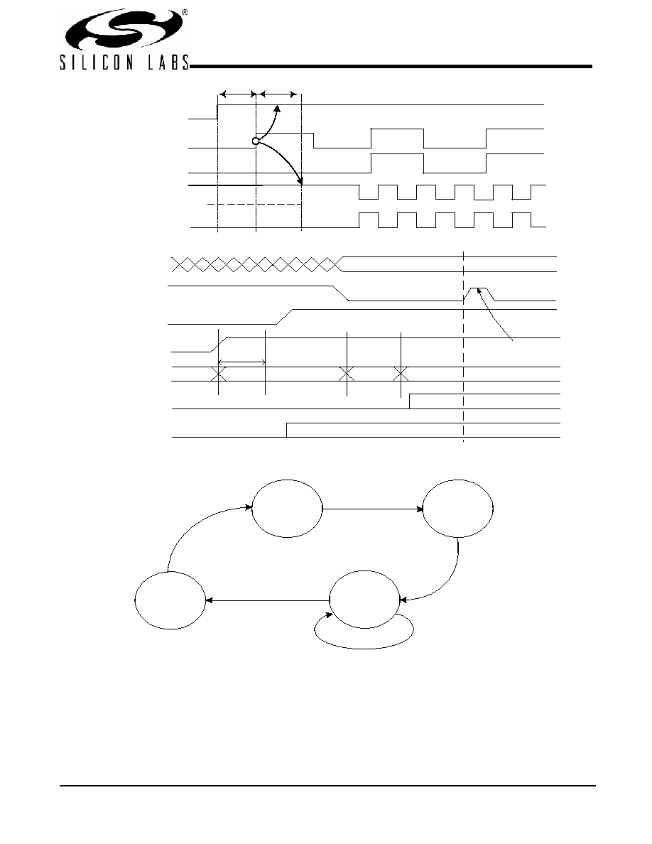
PCI_STP#
PCI_F
PCI
SRC 100MHz
Tsu
Tdrive_SRC
Figure 11. PCI_STP# Deassertion Waveform
FS_A, FS_B,FS_C
VTT_PW RGD#
PW RGD_VRM
VDD Clock Gen
Clock State
Clock Outputs
Clock VCO
0.2-0.3mS
Delay
State 0
State 2
State 3
Wait for
VTT_PW RGD#
Sample Sels
Off
On
State 1
Device is not affected,
VTT_PW RGD# is ignored
Figure 12. VTTPWRGD# Timing Diagram
VTT_PWRGD# = Low
Delay
>0.25mS
S1
Power Off
S0
VDD_A = 2.0V
Sample
Inputs straps
S2
Normal
Operation
Wait for <1.8ms
Enable Outputs
S3
VTT_PWRGD# = toggle
VDD_A = off
Figure 13. Clock Generator Power-up/Run State Diagram
发布紧急采购,3分钟左右您将得到回复。
相关PDF资料
CY28446LFXC
IC CLOCK CALISTOGA CK410M 64QFN
CY28447LFXC
IC CLOCK CALISTOGA CK410M 72QFN
CY28547LFXCT
IC CLOCK CK505/410M INTEL 72QFN
CY28548ZXC
IC CLK CK505 960M/965M 64TSSOP
CY28551LFXC-3T
IC CLOCK INTEL/AMD SIS VIA 56QFN
CY28551LFXC
IC CLOCK INTEL/AMD SIS VIA 64QFN
CY2SSTV855ZXI
IC CLOCK DIFFDRV PLL DDR 28TSSOP
CY2SSTV857ZXI-27
IC CLK DDR266/333BUF1:10 48TSSOP
相关代理商/技术参数
CY28445LFXC-5T
功能描述:时钟发生器及支持产品 Calistoga RoHS:否 制造商:Silicon Labs 类型:Clock Generators 最大输入频率:14.318 MHz 最大输出频率:166 MHz 输出端数量:16 占空比 - 最大:55 % 工作电源电压:3.3 V 工作电源电流:1 mA 最大工作温度:+ 85 C 安装风格:SMD/SMT 封装 / 箱体:QFN-56
CY28446
制造商:CYPRESS 制造商全称:Cypress Semiconductor 功能描述:Clock Generator for Intel㈢ Calistoga Chipset
CY28446LFXC
功能描述:时钟发生器及支持产品 Calistoga RoHS:否 制造商:Silicon Labs 类型:Clock Generators 最大输入频率:14.318 MHz 最大输出频率:166 MHz 输出端数量:16 占空比 - 最大:55 % 工作电源电压:3.3 V 工作电源电流:1 mA 最大工作温度:+ 85 C 安装风格:SMD/SMT 封装 / 箱体:QFN-56
CY28446LFXCT
功能描述:时钟发生器及支持产品 Calistoga RoHS:否 制造商:Silicon Labs 类型:Clock Generators 最大输入频率:14.318 MHz 最大输出频率:166 MHz 输出端数量:16 占空比 - 最大:55 % 工作电源电压:3.3 V 工作电源电流:1 mA 最大工作温度:+ 85 C 安装风格:SMD/SMT 封装 / 箱体:QFN-56
CY28447
制造商:SPECTRALINEAR 制造商全称:SPECTRALINEAR 功能描述:Clock Generator for Intel㈢ Calistoga Chipset
CY28447LFXC
功能描述:时钟发生器及支持产品 Calistoga System Clk Extra SRC Output RoHS:否 制造商:Silicon Labs 类型:Clock Generators 最大输入频率:14.318 MHz 最大输出频率:166 MHz 输出端数量:16 占空比 - 最大:55 % 工作电源电压:3.3 V 工作电源电流:1 mA 最大工作温度:+ 85 C 安装风格:SMD/SMT 封装 / 箱体:QFN-56
CY28447LFXCT
功能描述:时钟发生器及支持产品 Calistoga System Clk Extra SRC Output RoHS:否 制造商:Silicon Labs 类型:Clock Generators 最大输入频率:14.318 MHz 最大输出频率:166 MHz 输出端数量:16 占空比 - 最大:55 % 工作电源电压:3.3 V 工作电源电流:1 mA 最大工作温度:+ 85 C 安装风格:SMD/SMT 封装 / 箱体:QFN-56
CY28506OC
制造商:Rochester Electronics LLC 功能描述:FTG FOR MOTHERBOARDS - Bulk